
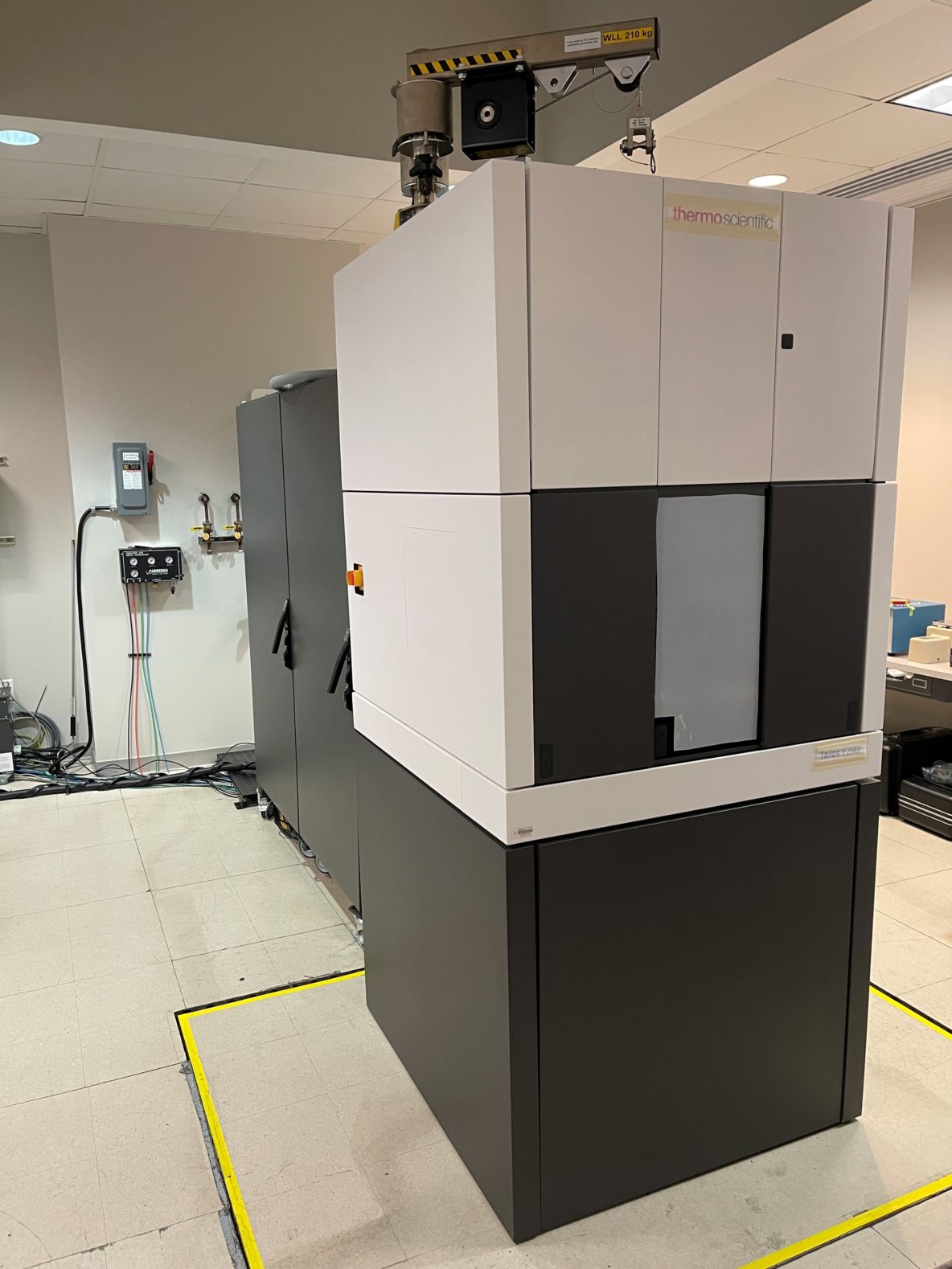
TFS Talos F200i Transmission Electron Microscope
Pricing
| $95/Hour | TAMU Users & Federal Government Agency Users |
| $70/Hour | Off-Peak & Automated Runs (TAMU Users & Federal Government Users only) 5:00 p.m. - 8:00 a.m. |
| $423/Hour | Other Universities and Industry |
Capabilities:
Analysis of morphology, crystallography, and composition of bulk and nanoscale materials.
Specifications:
Source:
- Ultra-high brightness cold field-emission-gun (X-CFEG) with X-Twin objective lens providing a superior energy resolution
- Fully computer-controlled and automated projector screen and apertures
Detector:
- Annular bright field (ABF) and high angle annular dark field (HAADF) Panther STEM detector
- Bruker Super-X EDS windowless detector with a detectability down to boron
Resolution:
- TEM information limit: ≤ 0.11 nm
- TEM line resolution: ≤ 0.10 nm
- STEM resolution: ≤ 0.14 nm
- EDS energy resolution: ≤ 140 eV
Magnification:
- TEM mode: 25 – 1.05 Mx
- STEM mode: 310 – 330 Mx
- Field of view: 2 ± 0.1 mm at zero degrees for both alpha and beta tilt
- Maximum diffraction angle: 24o
Field of View:
- TEM mode: 25 – 1.05 Mx
- STEM mode: 310 – 330 Mx
- Field of view: 2 ± 0.1 mm at zero degrees for both alpha and beta tilt
- Maximum diffraction angle: 24o
Operation Voltage: 80 and 200kV
Stage:
- Fully computer-controlled, eucentric side-entry, high stability CompuStage
- Single and double tilt specimen holders and heating and cooling holders
Camera:
- Ceta-S 4k x 4k CMOS camera
Software:
- Velox data acquisition and processing software
- Inspect 3D for tomographic reconstructions
- TEM/ STEM/ EDS tomography data acquisition software
- Avizo for EM systems (Materials Science)
for imaging services, training or other questions
please contact Dr. Hansoo Kim, luminesc@tamu.edu.
Helpful Hints:
To acquire good images on the TEM sample thickness should typically be ≲100nm.